At present, industrial products tend to be miniaturized, which brings new challenges to the precision data acquisition system. Designers must balance the solution size and power consumption of the whole system, and realize more accurate signal measurement under higher bandwidth.
This paper will discuss these challenges in detail, focusing on the role of analog-to-digital converter (ADC) in industrial systems.
ADC package size
Just as people's growing demand for consumer electronic products, people's demand for reducing the size and power consumption of industrial equipment is also increasing. As long as the function and performance of the product are not affected, users will give priority to smaller and lighter portable or semi portable data acquisition devices, because such devices are easier to use in the laboratory or outside. The miniaturized PLC plug-in module occupies less space in the control panel of the factory workshop. Secondly, the shelf space required for equipment inventory and spare parts spare inventory is less.
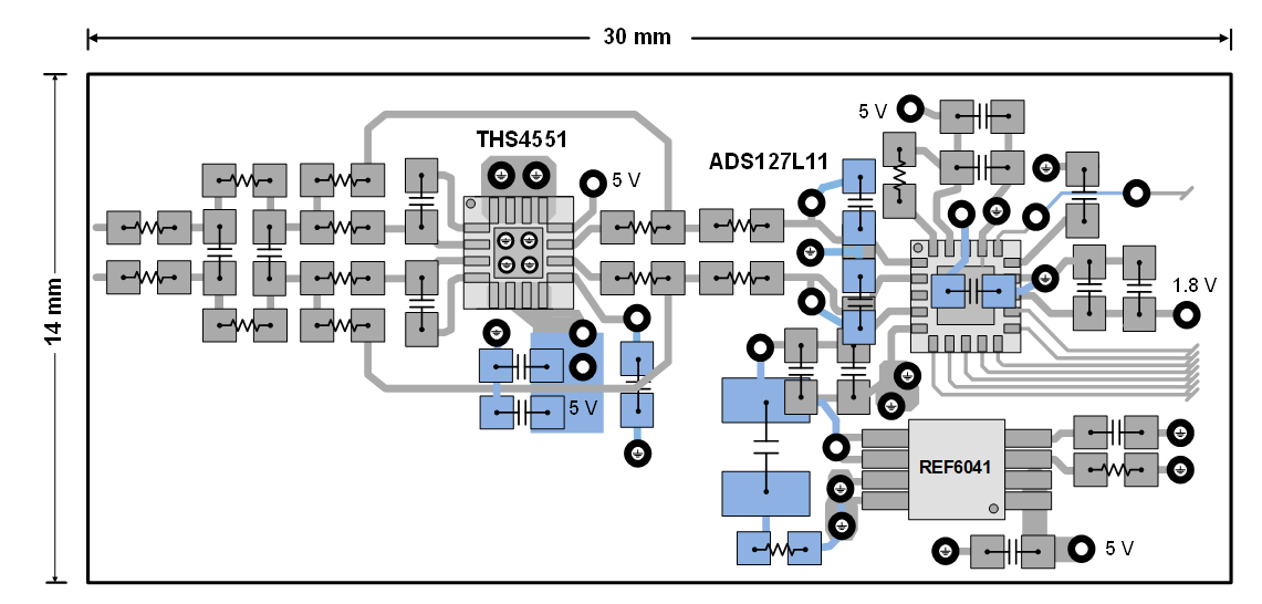
Of course, small product design is directly related to the size of internal electronic equipment. Figure 1 shows the layout of the data acquisition system, which uses Ti ths4551 full differential amplifier with fourth-order low-pass filter, ref6041 voltage reference with integrated buffer and ads127l11 broadband ADC. In view of the progress of new technology, it is worth noting that the converter is no longer the largest component in the design.

Figure 1: typical analog front-end printed circuit board (PCB) layout and wiring
ADC power consumption
Reducing power consumption to a greater extent is very important for prolonging the battery running time of portable devices. In addition, realizing low power consumption also means that smaller and lighter devices can be designed and the cost can be reduced as much as possible. For example, reduce four batteries in parallel to three.
Reducing power consumption can also benefit equipment powered off-line. Low power dissipation can reduce the temperature rise in the enclosure, thereby prolonging the product life by reducing the average junction temperature of integrated circuits (ICS) (in some cases, reducing or eliminating forced air cooling). In comparison, although removing the ventilation slot on the product shell or control panel can reduce the dust and steam accumulated on the surface area of the printed circuit board, it may cause problems in the field equipment if it is exposed to the harsh environment for a long time.
Reducing power consumption also means that the overall size of the magnetic components of the power supply is smaller. Of course, this size reduction also means that smaller enclosures can be selected.
ADC resolution
The source of noise will limit the measurement resolution in the data acquisition system (from the reference voltage and input signal conditioning circuit), but many satisfactory optional components can also help to minimize the impact of noise sources. It can be said that the main factor affecting the resolution of any industrial equipment system measuring AC signals (such as vibration / acoustic monitoring and general data acquisition) is the converter. The converter shall not have tones and other spurious frequencies that limit the measurement resolution, but shall have low broadband noise (which can solve small signal level) and low distortion, so as to achieve good spectrum performance.
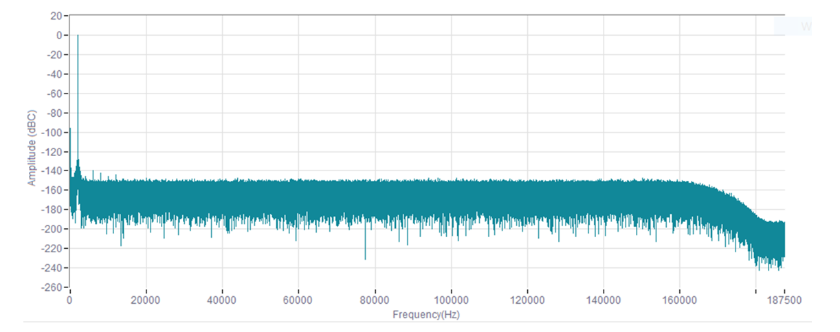
Fig. 2 is an example of good spectral performance of a precision data acquisition system. For the data shown in this example, the system elements used are also ths4551, ref6041 and ads127l11.

Figure 2: ADC spectrum performance
ADC bandwidth
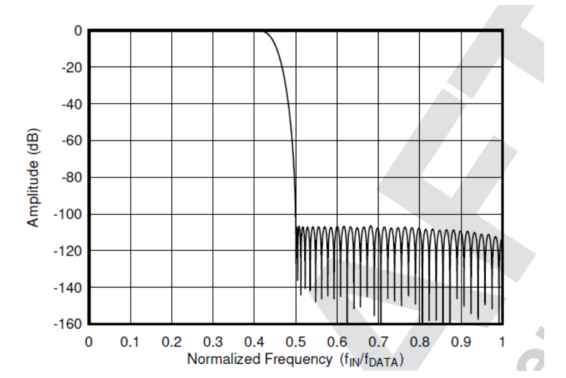
During accurate acquisition of AC signals, the converter should have near ideal frequency characteristics: low ripple flat passband, steep transition band (bandwidth can be saved as much as possible) and fully effective stopband at Nyquist frequency (signal aliasing can be reduced to a greater extent). In case of signal aliasing, the signal cannot be corrected by post-processing, so it is very important to attenuate the out of band signal as economically as possible.
broadband Δ-Σ ADC provides these filter characteristics, including key functions of anti aliasing. The broadband or brick wall filter is based on a digital filter having the above passband, transition band and stopband performance. The filter itself can only be realized by the concept of oversampling, and in order to obtain the ideal power and resolution index, it is usually compared with Δ-Σ Combined with ADC. Figure 3 shows the frequency response of a typical broadband ADC.

Figure 3: Broadband ADC filter response
Wideband filters have stopband attenuation and usually require a successive approximation register ADC without using an external anti aliasing filter. Both wideband filter and successive approximation register ADC can provide signal attenuation at Nyquist frequency. The equivalent order of the external anti aliasing filter will be very high and the implementation cost will be high. Avoiding the use of external filters can save design and component costs, and avoid a large number of in band phase shifts.

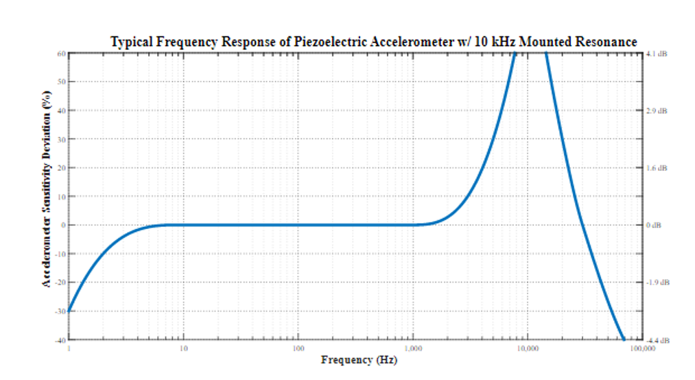
Figure 4: typical piezoelectric accelerometer with peak response under resonant conditions
The disadvantage of integrating broadband filter into converter is that many logic gates need to occupy silicon area in filter implementation. ADC IC designers can reduce power consumption by using small transistor size and associated low threshold voltage, but at the same time, analog friendly transistors are needed to achieve excellent analog partial noise and linear performance. Ti has developed IC processes that meet these two standards.
The small transistor geometry reduces the stray capacitance (c) associated with the logic gate, thereby reducing the internal power loss. Equation 1 represents the power loss (P) operating at clock frequency (f) and operating voltage (V):
P = V2 × f × C (1)
Reducing the threshold voltage reduces the power loss associated with the V2 power supply item. Another advantage is that the peak switching current is reduced through the small transistor size used in the ADC digital part, thereby reducing the noise of the digital switch coupled to the analog part.
epilogue
With the help of ads127l11, Ti designs a broadband ADC. Compared with the existing broadband converter, its package size is reduced by 50%, power consumption is reduced by 50%, resolution is improved by 3dB, and signal bandwidth is increased by 50%. Ads127l11 balances size and power factors without sacrificing resolution or bandwidth.
When choosing a precision broadband ADC, designers no longer need to choose between optimizing power consumption, package size, resolution and measurement bandwidth. Ti can meet the requirements of smaller and smaller dimensions, lower power consumption and higher resolution, so that you can easily choose converters for the next generation of data acquisition devices.