In the application of cordless electric tools, the voltage of the battery pack is usually 16V, 20V, 24V, 40V, 60V and 80V, and the mechanical switch will be used to control the driving board for power supply. However, due to the characteristics of the mechanical switch, there will be disadvantages such as switch spark, service life and volume. 
Figure 1: application of mechanical switches in power tools
The introduction of high side drive scheme in electric tools not only avoids the inherent shortcomings of traditional mechanical switches, but also has the advantages of strong controllability, adjustable conduction time, supporting multi packet parallel connection, short circuit protection, small volume and so on. As shown in Figure 2, the high side drive IC will generate a voltage 12V higher than the battery pack. By controlling the gate voltage of MOS, the on-off of the main circuit can be controlled.
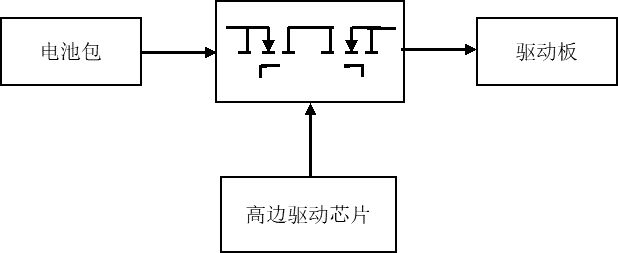
Figure 2: scheme of high side drive chip in electric tool
1. Lm5050 supporting multi packet parallel connection
The lm5050 is a high side oring FET Controller. The operating voltage supports 1V – 75V and the maximum withstand voltage supports 100V. Lm5050 detects the voltage on VDS and controls the voltage on VGS to realize the function of ideal diode. At the same time, because the lm5050 has integrated a charge pump, the supply voltage does not need to be higher than the battery pack voltage. In cordless electric tools, the overall battery capacity can be improved by multi pack parallel connection, and the parallel connection of battery packs with different voltage levels can also be realized. As shown in Fig. 3, multiple battery packs can be connected in parallel through the control of the lm5050 by outputting the source stage of the series MOS through the battery pack.
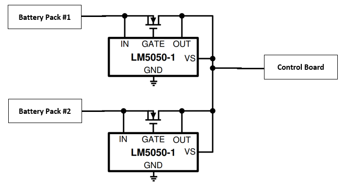
Figure 3: lm5050 application multi packet parallel scheme
2. Lm5060 supporting high side drive
Lm5060 is a high side protection controller. Its working voltage supports 5.5V - 65V. It supports overvoltage protection, undervoltage protection and overcurrent protection. It can be turned on and off by controlling the voltage of EN pin. The lm5060 is internally integrated with a charge pump and does not need additional power supply. It can realize 24ua gate charging current and 80mA gate discharge current. The power consumption of lm5060 is large, with working current of 1.4ma and disabling current of 9ua.
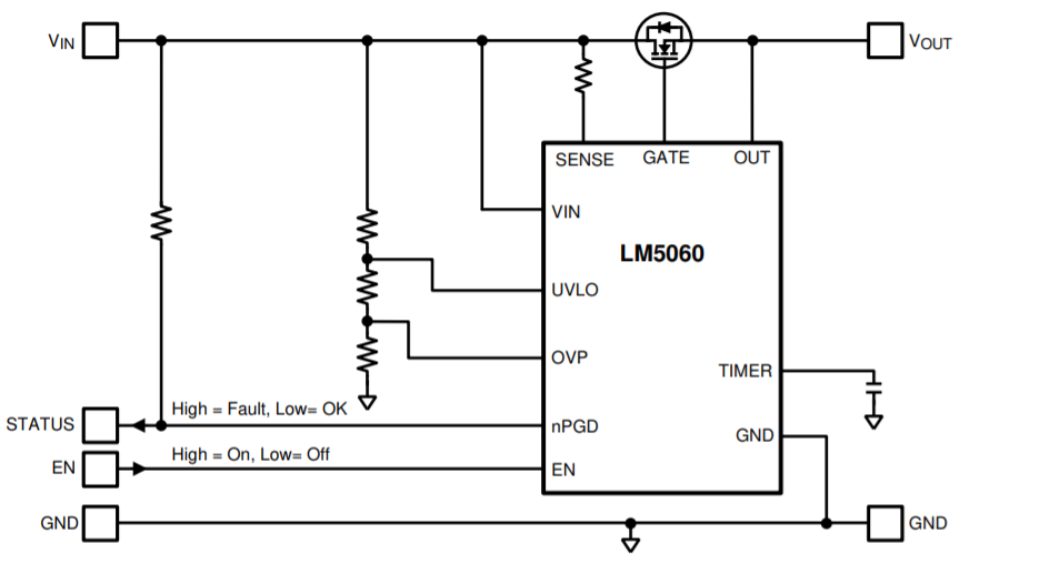
Figure 4: lm5060 high side drive scheme
3. Bq76200 supporting high side back to back MOS drive
Bq76200 is a high side nFET driver chip with working voltage of 8V – 75V and maximum withstand voltage of 100V. It can control two back to back MOS respectively. Compared with lm5060, the working current of bq76200 is 40ua. In the disabled state, the internal charge pump module will also be disabled. The static current does not exceed 10uA, which is more suitable for battery power supply system. At the same time, charging MOS and discharging MOS can be controlled independently, with higher flexibility.
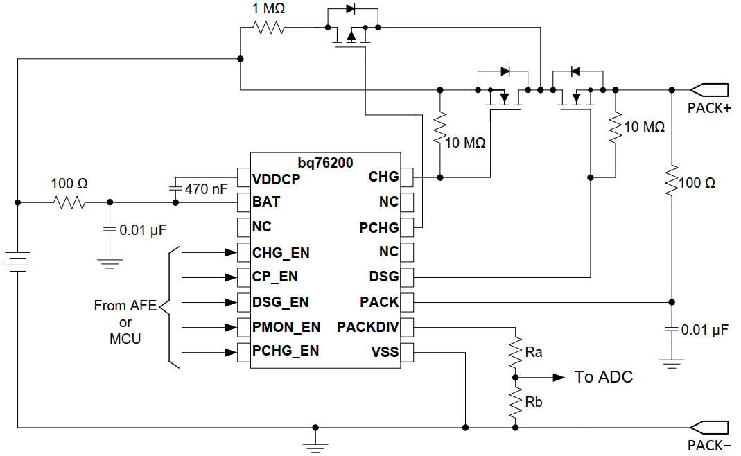
Figure 5: bq76200 supporting independent charge / discharge control
4. Lm7480x supporting ideal diode mode and output disconnection mode
Lm7480x is the driver of back to back nFET. It supports ideal diode mode and output disconnection control. The input voltage supports 3V – 65V and has - 65V reverse voltage bearing capacity. The driving on current is 20mA, the driving off current is 2.6a, the working current is 413ua, and the static current under failure is 2.87ua. The lm7480x has both the ideal diode mode of the lm5050 and the lm5060 output on-off control.
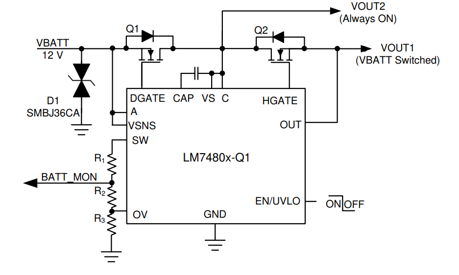
Figure 6: lm7480x supporting both ideal diode mode and output disconnect mode
5. Use half bridge driver chip to realize high side back to back nFET drive
For the previous drive IC, the battery voltage does not exceed 80V, the drive current is relatively small, and the switching speed is slow. For back to back nFET drivers above 80V, the scheme in Figure 6 (application report sluaa58) can be considered. As shown in Fig. 6, a charge pump is constructed through a half bridge drive chip, such as ucc27284, and the capacitance voltage of the charge pump is increased by 12V. The on-off of the power loop can be controlled by the logic level of the upper bridge arm. At the same time, the working current of general half bridge drive IC is large, and the working current reaches Ma level; The quiescent current is 7ua under the disabled condition. In terms of driving capacity, it depends on the charge pump capacitance and driving resistance as a whole. Under the conditions of supply voltage 12V, driving resistance 8.25 Ω and charge pump capacitance 470nf, the driving current is 1.68a and the on-off time is less than 0.5us.
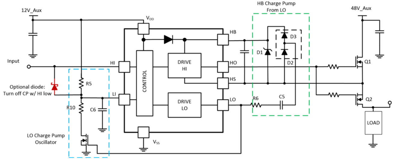
Figure 7: high side drive using half axle drive
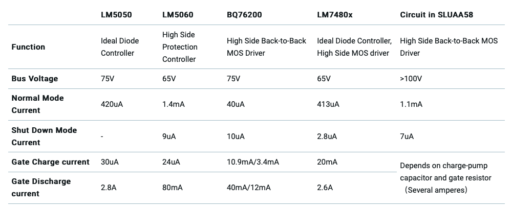
Finally, the comparison tables of the above five modes are given from the perspectives of bus voltage, function, driving capacity and static current.
Table 1: comparison of five high side driving modes
